Current Research
Bio-inspired color-tunable systems (2012-Present)
Tremendous progress has been made in display devices and virtual reality methods over the years, yet the primary representation remains “through the window”—we look, feel, or move using a computer interface that acts as a portal into a simulated world. Even with the best projection systems light emitting devices offer very limited simulations of the real world. There is a real need to explore novel material concepts in texture and color control to create physical manifestations of virtual objects. The major challenge for this revolution is the need of a new type of pixel that can change color and texture in a flexible substrate. Natural masterpieces such as the cuttlefish’s color- and texture-changing abilities prove that such technology is essentially possible, and that it is up to us to learn from nature’s blueprints. To that end we propose to comprehensively address the full opto-mechanical requirements to build structurally active designs to enable efficient color and texture surface control.
Natural nanoarchitectures such as the cuttlefish’s constitute a completely different ‘blueprint’ for realizing active structural color compatible with soft and flexible surfaces. We will pursue a technology based on soft materials to implement a controllable and flexible structural coloration scheme inspired by nature, which will come to life using low cost nano-replication technologies and will not consume energy to retain a state. It is important to point out that we are neither proposing that such technology would displace light emitting diode (LEDs) displays any time soon, nor other rigid and/or liquid-based architectures in development for the e-book reader market. What we are proposing here is fundamentally different, a technology based on intrinsically soft components that can really reproduce color and texture. It could have important implications in adaptive optics, camouflage, and the overall integration of visual and tactile experience in, for example, a truly artificial chameleonic skin. Our immediate objective is to demonstrate the physical feasibility of the key design and materials components behind this idea through understanding and optimization of the fundamental properties of nature-based photonic structures molded in dielectric elastomers in order to create angle-independent coloration that can be controlled with an electric field.

Materials/Photoanode for dye sensitized photoelectrochemical cells (DSPECs) (2009-Present)
Concerns about future limitations of the availability of hydrocarbons and the already ongoing global greenhouse problem continue to encourage the development of hydrogen as a carrier and storage medium of energy. In dye sensitized photoelectrochemical cell (DSPEC) applications, semiconductor requirements include high surface areas for adequate assembly loading, good transport properties (long carrier lifetimes relative to recombination), and a suitable energy band structure for promoting electron or hole injection for the latter, at potentials sufficient to drive hydrogen reduction at the counter electrode. We have developed a new pulsed laser deposition (PLD) method to fabricate candidate oxide photoanodes with a hierarchical and preferentially vertical arrangement. Given the nature of the fabrication process, morphology is largely independent of material and we have successfully applied PLD to the fabrication of high-potential conduction band oxides such as Nb2O5, SrTiO3 and Ta2O5. This is work that continues under the umbrella of the UNC-Energy Frontier Research Center.
Photonic Nanostructure of in Solar Cells (2007-Present)
Sunlight is the most abundant and sustainable source of energy available. However exploiting its concentrated fossil fuel forms has negative environmental and geopolitical consequences. Despite these known facts, societies do not price correctly the use of non-renewable fuel deposits, appearing the “cheapest” way to supply the world with energy. Despite this uphill situation, an economic upheaval in direct solar energy conversion technology seems possible. A technology can only have a chance of being disrupting if its costs are lower than that of comparable silicon cells and performs with commercial module photon conversion efficiencies (PCE) > 15 % (~20 % in laboratory). We advocate that sustainable energy research cannot be blind to these realities.
Clearly abundant and low cost materials are the only ones with a chance to surpass silicon’s cost trajectory. This is why we are committed to bet on alternative systems: namely organic, hybrid, and quantum dot solar cells. The key adversative problem –light absorption vs. carrier transport–, present in all types alternative photovoltaic materials is for most part being addressed on by improving the intrinsic characteristic of PV-active materials. As has been proven by Bulk Heterojunction devices the problem is surmountable by separating the absorption and transport issues and the key lies in identifying the correct length scales that need to be addressed.
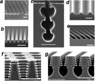
We are working on a program that pursues the conception and fabrication of integrally designed photonic solar cells. Our approach is based on the advanced optical control allowed via photonic crystals. The objective of this effort is to accomplish efficient light capturing by a photonic arrangement of nanostructures while at the same time significantly shortening the effective path that carriers must travel to reach the contacts. We are looking to build on that success and expand into other novel systems. Dye sensitized solar cells (DSSC) employ an organic dye to absorb light and inject electrons into a semiconductor oxide film. In order to accommodate enough dye molecules, a nanostructured large surface area is required for the oxide anode. Nonetheless, the film still needs to be ~10-15 μm thick to absorb a meaningful amount of light. This large thickness in turn presents considerable energy losses by increased serial resistance and recombination processes due to its commensurable electron diffusion length (< 10 μm). The fact that these two characteristic lengths are similar has allowed DSSCs to reach decent efficiencies but it has also prevented them from realizing their full potential. Our photonic “bush” photo-anode is being developed to revolutionize this impasse, with a great chance to be applied to other sensitizers as quantum dots.

Nanostructured photonic sensors (2008-Present)
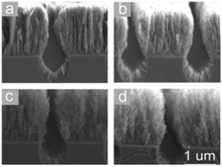
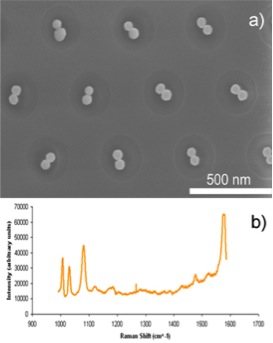
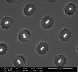
Another area where nanoscale features are having a revolutionary effect is in the field of sensor technology. The advent of laser and photon detection technologies has allowed Raman spectroscopy to become a practical tool to study analytes in bulk quantities. Today, under favorable (lucky) circumstances, surface enhanced Raman spectroscopy (SERS) is capable of single molecule detection which represents a ~1014 enhancement factor. This has prompted a renewed interest in this technique for a variety of applications ranging from security, chemical identification, environmental monitoring and healthcare. Although considerable progress has been made in elucidating the mechanisms behind SERS, SERS enhancements have not been reproduced at will in specific controlled locations. This standing problem is hardly surprising since theoretical and computational calculations have shown that the dominant field enhancements are specifically localized to the crevices between metal nanoparticles.
Our goal of this area is to address experimentally those theoretical predictions and create large area/low cost SERS substrates. In contrast to what other groups have done in the past, we are directing the metal nanoparticles to form only particle-dimers with controlled size, location and interparticle distance. We plan to arrive at definitive answers to the two fundamental questions.
Past Research
Photonic Hydrogen Detection (2007-2009)
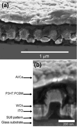
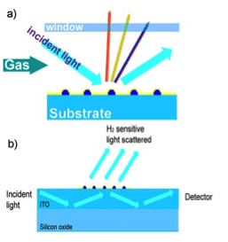
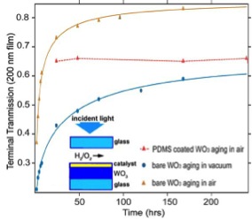
Currently there are H2 sensors on the market, the vast majority utilizing thin films made of palladium and/or metal transition oxides using their H2 sensitivity in electrical devices. For a number of applications these electrical devices are adequate, however, optical monitoring of hydrogen is considered the best method due to its safe nature compared with techniques requiring electrical measurements, i.e. in environments where the mixture might have reached explosive potential. Evidence of their more satisfactory performance lies in the fact that the number of hydrogen optical sensors has grown in recent years. However, all thin-film based hydrogen sensors have problems regarding speed and poisoning. The response time of these devices ranging from 0.5 s to several minutes is too slow to permit useful, real-time monitoring of flowing gas streams. In addition current devices quickly deteriorate in air. Our group has solved the poisoning problem in gasochromic WO3 films. We are targeting the speed/sensitivity issue. In principle, by using nanoscale structure, the time required for hydrogen atoms to diffusely equilibrate with this element can be reduced (more surface area, less volume). Furthermore, organizing the nanostructure in photonic crystals can give rise to higher sensitivity by maximizing the effect of the H2 induced change in optical constants. In this project we pursue the creation and fundamental scrutiny of photonic devices for detection of hydrogen.
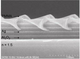
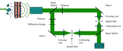
Plasmon amplification of evanescent waves (2009-2012)
In a conventional optical imaging system using lenses, transverse resolution is fundamentally limited by the diffraction limit, which is typically about half the wavelength of the light with a normal incidence exposure. This fundamental limit occurs when only propagating waves radiated by an object are collected, which is the case with a conventional imaging system using lenses. The key point in imaging with resolution below the diffraction limit lies on the collection and detection of both propagating and evanescent waves radiated by the object in the near field. A few years ago it was predicted that a simple planar thin film termed a superlens can be used to produce optical images with resolution below the diffraction limit. Optical imaging with resolution below the diffraction limit using a silver superlens was recently experimentally demonstrated. Although the use of a superlens is very promising for numerous possible applications, such as ultra-high density optical lithography, subwavelength sensing, nanofabrication, and related areas, imaging using the current superlens is limited in the near-field zone. We are working in an alternative way to overcome this limitation using a new device termed a far-field superlens, which is a properly designed periodically corrugated superlens. No one has proved this approach works experimentally, and we have started the fabrication of a device that comprises alternating layers of metal/dielectric and a diffraction grating.