Self-Organization
of a Carbide Superlattice on Mo (111)
It
has been widely known since the Industrial Revolution that adding small
amount
of carbon to many metals can improve their materials properties.
Recently the
same metals have been found to be the catalysts for synthesizing carbon
nanotubes, a new form of carbon. It has been speculated that the metal
catalyst
may need to be comparable in size compared to the diameter of the
nanotube in
order to serve as the nucleation site or the ‘root’, but the exact role
of the
catalyst is unclear. By studying deposition of small carbon clusters on
Mo
surface (a known nanotube catalyst), we observed the formation and
evolution of
ordered arrays of molybdenum carbide nanocrystals (i.e. carbide
superlattices)
on Mo (111) surface [Tsui & Ryan, Phys. Rev. Lett.
89,
015503 (2002); also J. Nanosci.
Tech.
(in press)]. The self-organization of the carbide nanocrystal arrays is
determined to be energetically driven, such that the crystalline
lattice
mismatch between carbide and Mo host determines the size and spacing of
the
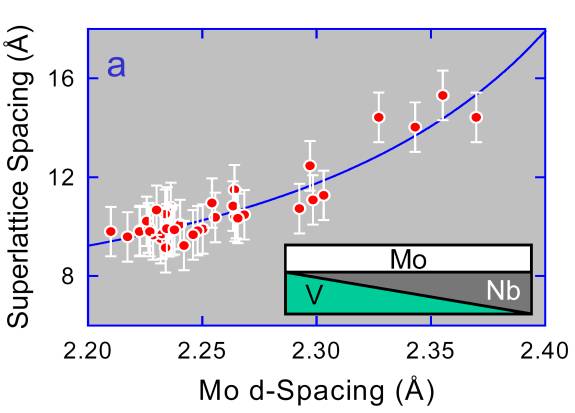
array, as illustrated in a
below. The
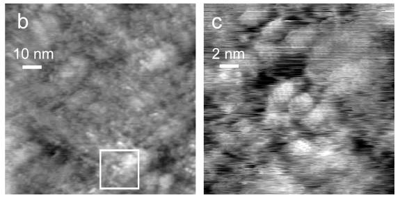
carbide nanocrystals appear to be the ‘roots’ for the carbon
precipitates, as
shown in STM images below (b
and c),
from which carbon nanotube ‘seedlings’ can
nucleate. This mechanism indicates that arrays of carbon nanotubes can
be grown
from large catalysts and it may open new opportunities for controlling
carbon
nanotube synthesis and for device applications.
a. Correlation
of lattice spacings
between molybdenum carbide superlattice and Mo (111), indicating
energetic
origin of the superlattice. Lattice spacing of the Mo host is ‘tuned’
by using
bcc metals of Nb and V (inset) with the former larger than Mo and
latter
smaller. The line is a fit using an energetic model based on
competition
between strain and surface energies
b & c. STM
images of initial carbon
precipitates on surface of the molybdenum carbide superlattice. The
precipitates resemble carbon nanotube
‘seedlings’, nucleation of carbon nanotubes. In b and c image sizes
are
100nm x 100nm and 20nm x 20nm,
respectively, and the box in b is the size
and
location of c.
|